From Graphene to Goldene: Advanced Single-Atom Layer Materials Open New Doors for Future Discoveries
None of us have any doubts about the value of gold in our minds. After all, it is the most popular and longstanding store of value. However, the scientific advances accomplished by human civilization have now taken us to the doorsteps of Goldene. And it could be a game-changer, to say the least. But what is Goldene? Why is the scientific community so excited about it? Let us delve deeper.
İçindekiler
Goldene: Sheets of Gold that is Only a Single Atom Layer Thick
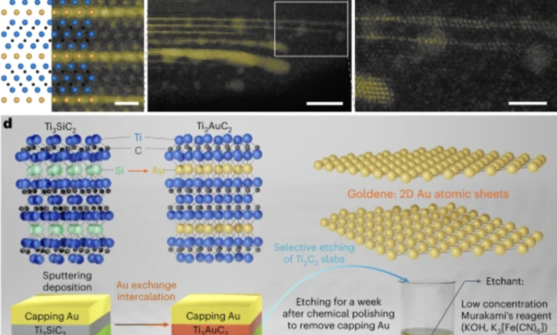
For the first time, researchers from Linköping University, Sweden, have created sheets of gold whose thickness is equal to a single atom layer. The researchers have named this derivation Goldene. Goldene may come in handy for a host of sophisticated tasks, including carbon dioxide conversion, hydrogen production, and the production of value-added chemicals.
According to Shun Kashiwaya, a researcher at the Materials Design Division at the University:
“If you make a material extremely thin, something extraordinary happens – as with graphene. The same thing happens with gold. As you know, gold is usually a metal, but if a single atom layer is thick, the gold can become a semiconductor instead.”
How Was ‘Goldene’ Created?
The invention started with the development of a three-dimensional base material created by embedding gold between layers of titanium and carbon. In high temperatures, the thinly layered silicon of Titanium Silicon Carbide was replaced by Gold, leading to the discovery of Titanium Gold Carbide. However, it was a chance discovery. The researchers were aiming to coat the electrically conductive titanium silicon carbide with gold so that it could make contact.
To carry out their job, the researchers leveraged a traditional method that has existed as a component of Japanese forging art for more than a hundred years now. The component is called Murakami’s reagent. The researchers used it in different concentrations and for different time spans to eventually reach the component.
While they could finally produce the gold sheets in the desired thickness of a single atom, it was crucial to get them stable. They used a tenside, a long molecule to separate and stabilize the sheets, as a surfactant to ensure that the sheets do not curl up.
While describing the final output and its scientific validation, Shun Kashiwaya, one of the researchers, had the following to say:
“The golden sheets are in a solution, a bit like cornflakes in milk. Using a type of “sieve,” we can collect the gold and examine it using an electron microscope to confirm that we have succeeded. Which we have.”
The Many Potential Applications of Goldene
Goldene’s potential applications span a wide range of fields, including carbon dioxide conversion, hydrogen-generating catalysis, selective production of value-added chemicals, hydrogen production, water purification, communication, and much more.
In the subsequent follow-up, the researchers plan to explore the possibility of reducing the amount of gold used in these applications and substituting gold with other noble metals. These new compounds might have many more new applications.
While Goldene promises to open up many new doors in terms of its scientific and technological applications, the scientific community’s fascination with single-layer atom materials is not new.
The Curious Case of Single-Layer Atom Materials: Graphene and More
Whenever we talk about single-layer atom materials, we necessarily discuss Graphene. It is popular because of its potential. Extracted from Graphite, carbon’s crystalline form, Graphene is light, elastic, and tough. Apart from its thinness, it has high resistance, 200 times more than steel. Yet, it is five times lighter than aluminum. It also has light absorption abilities and high electrical and thermal conductivity.
Graphene is more in discussion these days because of a breakthrough achieved recently where researchers could successfully demonstrate the first functional graphene semiconductor. This discovery may lead to dramatic changes in the world of computing and electronics.
While graphene could be the most popular and widely applicable single-layer atom material, there are several other examples in the category.
Single-layer atom materials are also known as 2D non-layered materials. They are named such because their formation happens by chemical bonding in three dimensions (3D), resulting in unsaturated dangling bonds on the surface and inducing a high-activity and high-energy surface.
Apart from Graphene, an example of one such single-layer material is black phosphorus, known as phosphorene. Among other non-layered materials, we have examples of silicone and germanene.
Owing to their layer-dependent properties, layer-edge effects, and variable band structures, these materials often exhibit a unique set of properties at their edges. They are modifiable by strain or applied electric fields, which also equip them with tuning properties.
Metal chalcogenides, metal oxides, III-V semiconductors, and organic-inorganic perovskites are among some of the most common single-layer atom or two-dimensional non-layered materials.
Let us briefly look into some of the real-life examples of such materials. Examples of Metal Chalcogenides include molybdenum disulphide (MoS2), tungsten disulphide (WS2), and tungsten diselenide (WSe2), while indium oxide (In2O3), tin oxide (SnO2), and zinc oxide (ZnO) are prime examples of metal oxides.
III-V semiconductors derive their name from the fact that they comprise a group III element, such as aluminum, gallium, or indium, bonded to a group V element, such as phosphorus, arsenic, or antimony. Gallium Arsenide and Indium Phosphate are examples of III-V semiconductors.
Examples of organic-inorganic perovskites include methyl ammonium lead iodide (MAPbI3) and formamidinium lead iodide (FAPbI3).
These materials could find several applications. There are businesses building solutions on them. In the forthcoming segment, we will look into them.
#1. Haydale Graphene Industries
The inert nature of Graphene made it difficult to adopt. Haydale Graphene Industries, to troubleshoot the issue, developed a powder-in, powder-out process that could seamlessly overcome this problem of plasma functionalization.
This process that could unleash the potential of Graphene became known as Haydale HDPlas, a dry, clean, and environmentally healthy method that could make graphene and other nanomaterials better by imparting them with the required mechanical strength and enhanced electrical and thermal conductivity.
Haydale has developed many interesting graphene-based solutions, including a range of customizable graphene inks for biomedical devices, flexible electronics, heating elements, and wearable technology. It is also a provider of functionalized boron nitride, known as white graphene. This synthetic ceramic material is non-toxic and can be found in solid and powder form. Some of its properties include insulation, strength, weight, and electrical conductivity.
Haydale’s portfolio of functionalized graphene and nanomaterial additives also proves effective in elastomer product manufacturing. These could be used in rubber bicycle and road tires, footwear rubber soles, seals, and gaskets. The Silicon Carbide graphene products of Haydale are used in ceramic-polymer surface treatment to protect concrete products.
Using graphene, Haydale has also developed useful composites, thermoplastics, and solar cutting tools.
Recently Haydale (AIM: HAYD) announced its Interim results for the year ended 31 December 2023 (“FY23”). According to the report, its Group Revenues increased by 38% to £2.47 million (H1 FY23 £1.78 million).
#2. Siemens
Another highly advanced use case for graphene foils could be seen in Siemens’ building of cyclotrons. A group of researchers utilized graphene foils as an extractor (stripper) foil in the 11-MeV Siemens Eclipse Cyclotron.
These foils exhibited exceptionally high thermal conductivity compared to carbon and significant mechanical strength. Their lifespan was more than 16,000 PA*H. The use of graphene foils also resulted in a significant increase in the transmission factor—the ratio of the beam current on the stripper foil to the current on the target—which was more than 90%.
The experiment showed how single-atom-layer graphene foils could efficiently compete with other carbon foils, which are usually used as stripper foils.
Siemens is known across the world for manufacturing high-end, sophisticated, and technology-intensive products. Such a company using single-layer atom materials in foil form shows the potential of the category.
In FY 2023, Siemens earned a revenue of 19.66 billion Euros, a notable increase from 17.39 billion Euros recorded in 2022.
More Explorations Around Single-Atom Layer Materials
Recent research showed that, in addition to materials like Goldene or Graphene, monolayer Black Phosphorus, also known as Phosphorene, offers distinct advantages in sensing applications. Scientists and researchers attribute these unique benefits to Phosphorene’s “puckered” lattice structure, which imparts the material with a larger surface-to-volume ratio than graphene and transition metal dichalcogenides (TMDCs). Phosphorene is versatile in its applications and can be used in various sensing scenarios, including gas sensing, humidity sensing, photo-detection, bio-sensing, and ion-sensing.
Phosphorene also shows considerable promise in electronics and optoelectronics. Scientific publications have revealed that its intrinsically anisotropic electronic, transport, optoelectronic, thermoelectric, and mechanical properties differ markedly from those of graphene and transition-metal dichalcogenides. The ease of fabrication and novel properties of phosphorene have spurred the design and demonstration of new nanodevices.
Another study pointed to the benefits of combining graphene and phosphorene. To delve deeper into how this combination could prove useful, we look into the comparative standings of sodium-ion batteries as an alternative to lithium-ion batteries. While sodium-ion batteries exhibit performances comparable to their lithium-ion counterparts, the challenge lies in developing more viable anode materials. And this is where the graphene-phosphorene combination comes into play.
In a scientific experiment, the researchers demonstrated its potential. A hybrid material made out of a few phosphorene layers sandwiched between graphene layers could show a specific capacity of 2,440 mA h g−1 (calculated using the mass of phosphorus only) at a current density of 0.05 A g−1 and an 83% capacity retention after 100 cycles while operating between 0 and 1.5 V.
The researchers used in situ transmission electron microscopy and ex-situ X-ray diffraction techniques to explain the large capacity of the anode they developed. They developed it through a dual mechanism of sodium ions intercalating along the x-axis of the phosphorene layers, followed by the formation of a Na3P alloy.
Another single-atom layer material that has successfully captured the scientific community’s imagination is Germanene. Interest in Germanene is primarily for its optical properties. The relevant calculation has shown that the Germanene sheet has significant light absorption in the solar spectrum and shows optical anisotropy.
Germanene is unique because it is a semiconductor with zero band gap and linear band dispersion around the K point. While the band gap opening occurs in the presence of bias voltage, it increases linearly with the increasing bias voltage strength.
Therefore, not just goldene but a host of single-atom layer materials, including graphene, phosphorene, germanene, and more, are about to open up new scientific frontiers for future discoveries.
We must keep our focus steady on the properties of these materials. Only then will we be able to discover more applications. We must remember that the high surface activity of 2D non-layered materials makes them useful catalysts for crucial reactions, such as the oxidation of carbon dioxide and the reduction of water.
These materials have proven their worth in energy storage and conversion by helping to devise fuel cells and solar cells. In optoelectronics, their properties result in the production of high-quality light-emitting diodes, lasers, and sensors. Their topological insulation properties also help make insulators that conduct electricity on their surface but insulate in bulk.
Altogether, advanced single-atom layer materials are gateways to a multitude of opportunities. In the future, we will witness widespread adoption for sure!
Click for the list of five companies leading the development of nanotechnology.